Silicon Carbide (SiC): The Wide-Bandgap Semiconductor Revolutionizing Power Electronics and Extreme-Environment Technologies green silicon carbide

1. Fundamental Features and Crystallographic Variety of Silicon Carbide
1.1 Atomic Structure and Polytypic Intricacy
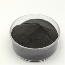
(Silicon Carbide Powder)
Silicon carbide (SiC) is a binary substance composed of silicon and carbon atoms prepared in an extremely stable covalent lattice, differentiated by its outstanding solidity, thermal conductivity, and electronic properties.
Unlike conventional semiconductors such as silicon or germanium, SiC does not exist in a solitary crystal framework yet shows up in over 250 distinct polytypes– crystalline types that vary in the piling series of silicon-carbon bilayers along the c-axis.
The most technologically pertinent polytypes consist of 3C-SiC (cubic, zincblende framework), 4H-SiC, and 6H-SiC (both hexagonal), each displaying subtly different electronic and thermal features.
Among these, 4H-SiC is specifically favored for high-power and high-frequency digital gadgets because of its higher electron movement and reduced on-resistance compared to various other polytypes.
The solid covalent bonding– consisting of roughly 88% covalent and 12% ionic personality– confers remarkable mechanical strength, chemical inertness, and resistance to radiation damages, making SiC suitable for procedure in extreme atmospheres.
1.2 Digital and Thermal Features
The digital superiority of SiC originates from its large bandgap, which ranges from 2.3 eV (3C-SiC) to 3.3 eV (4H-SiC), considerably bigger than silicon’s 1.1 eV.
This vast bandgap enables SiC gadgets to operate at much higher temperatures– as much as 600 ° C– without intrinsic provider generation frustrating the gadget, a crucial restriction in silicon-based electronic devices.
Additionally, SiC possesses a high critical electrical area stamina (~ 3 MV/cm), about 10 times that of silicon, enabling thinner drift layers and greater malfunction voltages in power tools.
Its thermal conductivity (~ 3.7– 4.9 W/cm · K for 4H-SiC) surpasses that of copper, facilitating effective heat dissipation and lowering the requirement for complex cooling systems in high-power applications.
Incorporated with a high saturation electron velocity (~ 2 × 10 seven cm/s), these buildings make it possible for SiC-based transistors and diodes to change faster, manage higher voltages, and run with greater energy effectiveness than their silicon equivalents.
These features collectively place SiC as a fundamental product for next-generation power electronics, specifically in electrical automobiles, renewable resource systems, and aerospace innovations.

( Silicon Carbide Powder)
2. Synthesis and Fabrication of High-Quality Silicon Carbide Crystals
2.1 Mass Crystal Growth via Physical Vapor Transportation
The manufacturing of high-purity, single-crystal SiC is one of one of the most difficult elements of its technological implementation, primarily because of its high sublimation temperature (~ 2700 ° C )and complicated polytype control.
The leading approach for bulk growth is the physical vapor transportation (PVT) technique, likewise referred to as the changed Lely method, in which high-purity SiC powder is sublimated in an argon atmosphere at temperatures going beyond 2200 ° C and re-deposited onto a seed crystal.
Exact control over temperature slopes, gas flow, and pressure is important to lessen issues such as micropipes, misplacements, and polytype incorporations that degrade tool performance.
Despite developments, the development price of SiC crystals remains slow– commonly 0.1 to 0.3 mm/h– making the process energy-intensive and expensive compared to silicon ingot manufacturing.
Continuous research concentrates on maximizing seed positioning, doping harmony, and crucible layout to improve crystal high quality and scalability.
2.2 Epitaxial Layer Deposition and Device-Ready Substratums
For electronic device fabrication, a slim epitaxial layer of SiC is expanded on the bulk substratum using chemical vapor deposition (CVD), typically using silane (SiH ₄) and propane (C THREE H EIGHT) as precursors in a hydrogen atmosphere.
This epitaxial layer needs to exhibit specific density control, reduced problem thickness, and tailored doping (with nitrogen for n-type or aluminum for p-type) to form the active regions of power devices such as MOSFETs and Schottky diodes.
The lattice mismatch in between the substrate and epitaxial layer, in addition to residual stress from thermal growth differences, can introduce stacking mistakes and screw dislocations that impact gadget reliability.
Advanced in-situ tracking and process optimization have considerably decreased problem densities, making it possible for the industrial manufacturing of high-performance SiC tools with long functional life times.
Additionally, the development of silicon-compatible handling techniques– such as dry etching, ion implantation, and high-temperature oxidation– has actually helped with combination into existing semiconductor production lines.
3. Applications in Power Electronic Devices and Energy Systems
3.1 High-Efficiency Power Conversion and Electric Mobility
Silicon carbide has become a keystone material in contemporary power electronic devices, where its ability to switch at high regularities with minimal losses converts into smaller, lighter, and much more effective systems.
In electrical automobiles (EVs), SiC-based inverters convert DC battery power to air conditioner for the electric motor, running at frequencies up to 100 kHz– dramatically greater than silicon-based inverters– reducing the size of passive parts like inductors and capacitors.
This leads to increased power thickness, expanded driving variety, and boosted thermal management, directly addressing key difficulties in EV style.
Significant vehicle manufacturers and distributors have adopted SiC MOSFETs in their drivetrain systems, accomplishing power financial savings of 5– 10% compared to silicon-based services.
In a similar way, in onboard chargers and DC-DC converters, SiC gadgets allow quicker charging and greater performance, accelerating the change to lasting transportation.
3.2 Renewable Resource and Grid Facilities
In photovoltaic or pv (PV) solar inverters, SiC power modules boost conversion performance by lowering switching and transmission losses, especially under partial tons conditions common in solar energy generation.
This enhancement raises the overall power yield of solar installments and lowers cooling requirements, reducing system expenses and enhancing integrity.
In wind generators, SiC-based converters manage the variable frequency result from generators extra successfully, making it possible for much better grid assimilation and power quality.
Past generation, SiC is being deployed in high-voltage direct present (HVDC) transmission systems and solid-state transformers, where its high malfunction voltage and thermal stability support portable, high-capacity power distribution with very little losses over fars away.
These advancements are crucial for improving aging power grids and fitting the expanding share of dispersed and intermittent eco-friendly resources.
4. Arising Duties in Extreme-Environment and Quantum Technologies
4.1 Procedure in Rough Conditions: Aerospace, Nuclear, and Deep-Well Applications
The effectiveness of SiC expands beyond electronic devices into settings where traditional products fail.
In aerospace and defense systems, SiC sensing units and electronics run dependably in the high-temperature, high-radiation problems near jet engines, re-entry cars, and area probes.
Its radiation solidity makes it perfect for atomic power plant tracking and satellite electronics, where exposure to ionizing radiation can break down silicon gadgets.
In the oil and gas industry, SiC-based sensing units are made use of in downhole boring tools to endure temperature levels exceeding 300 ° C and destructive chemical environments, allowing real-time data purchase for enhanced extraction performance.
These applications leverage SiC’s capability to maintain architectural stability and electric capability under mechanical, thermal, and chemical stress.
4.2 Integration right into Photonics and Quantum Sensing Platforms
Beyond timeless electronic devices, SiC is becoming an encouraging platform for quantum innovations because of the existence of optically active factor flaws– such as divacancies and silicon jobs– that exhibit spin-dependent photoluminescence.
These issues can be manipulated at area temperature level, functioning as quantum bits (qubits) or single-photon emitters for quantum interaction and sensing.
The vast bandgap and low inherent service provider concentration allow for long spin comprehensibility times, essential for quantum data processing.
Moreover, SiC is compatible with microfabrication methods, enabling the combination of quantum emitters into photonic circuits and resonators.
This mix of quantum capability and industrial scalability settings SiC as an unique material linking the void between fundamental quantum scientific research and sensible device design.
In summary, silicon carbide represents a standard shift in semiconductor innovation, offering exceptional efficiency in power effectiveness, thermal monitoring, and ecological durability.
From enabling greener power systems to supporting expedition precede and quantum realms, SiC remains to redefine the restrictions of what is technically feasible.
Vendor
RBOSCHCO is a trusted global chemical material supplier & manufacturer with over 12 years experience in providing super high-quality chemicals and Nanomaterials. The company export to many countries, such as USA, Canada, Europe, UAE, South Africa, Tanzania, Kenya, Egypt, Nigeria, Cameroon, Uganda, Turkey, Mexico, Azerbaijan, Belgium, Cyprus, Czech Republic, Brazil, Chile, Argentina, Dubai, Japan, Korea, Vietnam, Thailand, Malaysia, Indonesia, Australia,Germany, France, Italy, Portugal etc. As a leading nanotechnology development manufacturer, RBOSCHCO dominates the market. Our professional work team provides perfect solutions to help improve the efficiency of various industries, create value, and easily cope with various challenges. If you are looking for green silicon carbide, please send an email to: sales1@rboschco.com
Tags: silicon carbide,silicon carbide mosfet,mosfet sic
All articles and pictures are from the Internet. If there are any copyright issues, please contact us in time to delete.
Inquiry us