Molybdenum Disulfide: A Two-Dimensional Transition Metal Dichalcogenide at the Frontier of Solid Lubrication, Electronics, and Quantum Materials mos2 powder

1. Crystal Framework and Split Anisotropy
1.1 The 2H and 1T Polymorphs: Structural and Electronic Duality
(Molybdenum Disulfide)
Molybdenum disulfide (MoS TWO) is a split transition metal dichalcogenide (TMD) with a chemical formula containing one molybdenum atom sandwiched between two sulfur atoms in a trigonal prismatic sychronisation, developing covalently bound S– Mo– S sheets.
These specific monolayers are stacked up and down and held together by weak van der Waals forces, allowing easy interlayer shear and exfoliation to atomically thin two-dimensional (2D) crystals– a structural attribute central to its varied useful functions.
MoS ₂ exists in numerous polymorphic forms, one of the most thermodynamically secure being the semiconducting 2H stage (hexagonal proportion), where each layer exhibits a straight bandgap of ~ 1.8 eV in monolayer type that transitions to an indirect bandgap (~ 1.3 eV) in bulk, a phenomenon critical for optoelectronic applications.
On the other hand, the metastable 1T stage (tetragonal balance) takes on an octahedral control and behaves as a metal conductor due to electron contribution from the sulfur atoms, enabling applications in electrocatalysis and conductive composites.
Stage transitions between 2H and 1T can be induced chemically, electrochemically, or through strain engineering, offering a tunable system for developing multifunctional devices.
The capability to stabilize and pattern these stages spatially within a solitary flake opens paths for in-plane heterostructures with distinct digital domains.
1.2 Problems, Doping, and Edge States
The efficiency of MoS ₂ in catalytic and electronic applications is highly sensitive to atomic-scale problems and dopants.
Intrinsic factor defects such as sulfur vacancies serve as electron contributors, enhancing n-type conductivity and functioning as energetic websites for hydrogen development responses (HER) in water splitting.
Grain boundaries and line defects can either impede charge transport or develop local conductive pathways, depending upon their atomic arrangement.
Managed doping with change metals (e.g., Re, Nb) or chalcogens (e.g., Se) permits fine-tuning of the band structure, carrier concentration, and spin-orbit combining effects.
Significantly, the edges of MoS two nanosheets, specifically the metal Mo-terminated (10– 10) edges, show considerably higher catalytic task than the inert basal airplane, inspiring the design of nanostructured drivers with taken full advantage of side exposure.
( Molybdenum Disulfide)
These defect-engineered systems exhibit just how atomic-level manipulation can change a normally taking place mineral into a high-performance useful product.
2. Synthesis and Nanofabrication Methods
2.1 Bulk and Thin-Film Manufacturing Techniques
Natural molybdenite, the mineral type of MoS ₂, has been made use of for decades as a solid lube, yet modern-day applications require high-purity, structurally regulated artificial kinds.
Chemical vapor deposition (CVD) is the leading method for creating large-area, high-crystallinity monolayer and few-layer MoS two films on substrates such as SiO ₂/ Si, sapphire, or versatile polymers.
In CVD, molybdenum and sulfur forerunners (e.g., MoO three and S powder) are vaporized at heats (700– 1000 ° C )under controlled atmospheres, enabling layer-by-layer development with tunable domain dimension and positioning.
Mechanical peeling (“scotch tape approach”) continues to be a criteria for research-grade examples, generating ultra-clean monolayers with very little defects, though it does not have scalability.
Liquid-phase exfoliation, entailing sonication or shear blending of mass crystals in solvents or surfactant remedies, generates colloidal dispersions of few-layer nanosheets appropriate for coverings, compounds, and ink formulations.
2.2 Heterostructure Integration and Device Patterning
Real potential of MoS two emerges when incorporated into vertical or lateral heterostructures with various other 2D materials such as graphene, hexagonal boron nitride (h-BN), or WSe two.
These van der Waals heterostructures make it possible for the style of atomically specific tools, consisting of tunneling transistors, photodetectors, and light-emitting diodes (LEDs), where interlayer cost and energy transfer can be engineered.
Lithographic pattern and etching methods enable the construction of nanoribbons, quantum dots, and field-effect transistors (FETs) with channel sizes down to 10s of nanometers.
Dielectric encapsulation with h-BN safeguards MoS ₂ from environmental destruction and reduces fee spreading, dramatically enhancing service provider movement and tool stability.
These manufacture advancements are crucial for transitioning MoS ₂ from research laboratory inquisitiveness to feasible element in next-generation nanoelectronics.
3. Practical Features and Physical Mechanisms
3.1 Tribological Actions and Solid Lubrication
Among the oldest and most enduring applications of MoS two is as a completely dry strong lube in severe environments where liquid oils fall short– such as vacuum, high temperatures, or cryogenic problems.
The low interlayer shear toughness of the van der Waals gap enables easy sliding in between S– Mo– S layers, causing a coefficient of rubbing as low as 0.03– 0.06 under ideal problems.
Its performance is even more boosted by solid attachment to steel surface areas and resistance to oxidation up to ~ 350 ° C in air, beyond which MoO four formation enhances wear.
MoS two is commonly utilized in aerospace mechanisms, vacuum pumps, and weapon parts, typically used as a layer using burnishing, sputtering, or composite consolidation right into polymer matrices.
Current researches show that moisture can break down lubricity by raising interlayer bond, motivating research study into hydrophobic finishings or crossbreed lubes for improved environmental stability.
3.2 Digital and Optoelectronic Feedback
As a direct-gap semiconductor in monolayer kind, MoS ₂ exhibits solid light-matter interaction, with absorption coefficients surpassing 10 ⁵ centimeters ⁻¹ and high quantum return in photoluminescence.
This makes it optimal for ultrathin photodetectors with rapid reaction times and broadband sensitivity, from visible to near-infrared wavelengths.
Field-effect transistors based on monolayer MoS ₂ demonstrate on/off proportions > 10 eight and service provider flexibilities as much as 500 centimeters TWO/ V · s in suspended samples, though substrate interactions typically restrict useful worths to 1– 20 cm ²/ V · s.
Spin-valley combining, an effect of solid spin-orbit communication and damaged inversion symmetry, enables valleytronics– an unique standard for details encoding utilizing the valley level of flexibility in energy room.
These quantum phenomena setting MoS two as a candidate for low-power logic, memory, and quantum computer components.
4. Applications in Power, Catalysis, and Emerging Technologies
4.1 Electrocatalysis for Hydrogen Development Response (HER)
MoS ₂ has become an appealing non-precious alternative to platinum in the hydrogen development reaction (HER), a crucial process in water electrolysis for environment-friendly hydrogen manufacturing.
While the basal plane is catalytically inert, side sites and sulfur openings exhibit near-optimal hydrogen adsorption free power (ΔG_H * ≈ 0), similar to Pt.
Nanostructuring techniques– such as producing vertically straightened nanosheets, defect-rich movies, or doped crossbreeds with Ni or Co– take full advantage of energetic website thickness and electric conductivity.
When integrated into electrodes with conductive supports like carbon nanotubes or graphene, MoS ₂ achieves high existing densities and lasting security under acidic or neutral conditions.
Additional enhancement is accomplished by stabilizing the metallic 1T stage, which improves intrinsic conductivity and reveals added active websites.
4.2 Adaptable Electronic Devices, Sensors, and Quantum Gadgets
The mechanical versatility, openness, and high surface-to-volume ratio of MoS two make it excellent for versatile and wearable electronic devices.
Transistors, logic circuits, and memory gadgets have been shown on plastic substratums, making it possible for bendable display screens, wellness monitors, and IoT sensors.
MoS ₂-based gas sensors exhibit high sensitivity to NO TWO, NH TWO, and H TWO O as a result of bill transfer upon molecular adsorption, with action times in the sub-second variety.
In quantum innovations, MoS two hosts localized excitons and trions at cryogenic temperature levels, and strain-induced pseudomagnetic fields can catch carriers, enabling single-photon emitters and quantum dots.
These growths highlight MoS two not just as a functional product however as a system for exploring fundamental physics in minimized dimensions.
In summary, molybdenum disulfide exhibits the merging of classic materials scientific research and quantum engineering.
From its old function as a lubricant to its modern deployment in atomically slim electronic devices and energy systems, MoS ₂ continues to redefine the limits of what is possible in nanoscale products layout.
As synthesis, characterization, and assimilation methods breakthrough, its influence across scientific research and innovation is positioned to increase also further.
5. Supplier
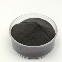
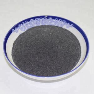
TRUNNANO is a globally recognized Molybdenum Disulfide manufacturer and supplier of compounds with more than 12 years of expertise in the highest quality nanomaterials and other chemicals. The company develops a variety of powder materials and chemicals. Provide OEM service. If you need high quality Molybdenum Disulfide, please feel free to contact us. You can click on the product to contact us.
Tags: Molybdenum Disulfide, nano molybdenum disulfide, MoS2
All articles and pictures are from the Internet. If there are any copyright issues, please contact us in time to delete.
Inquiry us