Alumina Ceramic Substrates: The Foundational Enablers of High-Performance Electronic Packaging and Microsystem Integration in Modern Technology alumina castable
1. Material Principles and Architectural Attributes of Alumina Ceramics
1.1 Crystallographic and Compositional Basis of α-Alumina
(Alumina Ceramic Substrates)
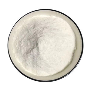
Alumina ceramic substratums, mainly composed of light weight aluminum oxide (Al two O ₃), work as the foundation of modern-day digital product packaging as a result of their extraordinary balance of electric insulation, thermal security, mechanical toughness, and manufacturability.
One of the most thermodynamically secure phase of alumina at heats is corundum, or α-Al ₂ O FIVE, which takes shape in a hexagonal close-packed oxygen latticework with aluminum ions inhabiting two-thirds of the octahedral interstitial sites.
This thick atomic arrangement conveys high hardness (Mohs 9), outstanding wear resistance, and strong chemical inertness, making α-alumina suitable for harsh operating settings.
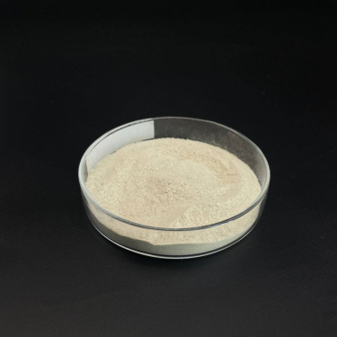
Business substratums typically consist of 90– 99.8% Al ₂ O SIX, with small enhancements of silica (SiO TWO), magnesia (MgO), or unusual planet oxides made use of as sintering aids to promote densification and control grain growth throughout high-temperature processing.
Higher pureness grades (e.g., 99.5% and over) show exceptional electric resistivity and thermal conductivity, while lower pureness versions (90– 96%) use cost-efficient solutions for much less demanding applications.
1.2 Microstructure and Problem Engineering for Electronic Integrity
The performance of alumina substratums in digital systems is critically depending on microstructural harmony and issue minimization.
A fine, equiaxed grain framework– typically ranging from 1 to 10 micrometers– makes sure mechanical integrity and minimizes the likelihood of split breeding under thermal or mechanical stress.
Porosity, particularly interconnected or surface-connected pores, must be reduced as it weakens both mechanical stamina and dielectric efficiency.
Advanced processing strategies such as tape casting, isostatic pushing, and regulated sintering in air or controlled atmospheres make it possible for the production of substratums with near-theoretical density (> 99.5%) and surface roughness listed below 0.5 µm, vital for thin-film metallization and cord bonding.
Additionally, impurity partition at grain limits can bring about leakage currents or electrochemical movement under predisposition, necessitating rigorous control over basic material pureness and sintering problems to make sure lasting dependability in damp or high-voltage atmospheres.
2. Production Processes and Substrate Manufacture Technologies
( Alumina Ceramic Substrates)
2.1 Tape Casting and Eco-friendly Body Handling
The manufacturing of alumina ceramic substratums starts with the prep work of a highly spread slurry consisting of submicron Al ₂ O three powder, natural binders, plasticizers, dispersants, and solvents.
This slurry is processed using tape spreading– a continuous technique where the suspension is spread over a moving service provider movie utilizing an accuracy medical professional blade to accomplish uniform thickness, generally in between 0.1 mm and 1.0 mm.
After solvent evaporation, the resulting “eco-friendly tape” is flexible and can be punched, pierced, or laser-cut to develop using holes for vertical affiliations.
Multiple layers might be laminated flooring to create multilayer substratums for intricate circuit assimilation, although most of industrial applications make use of single-layer setups due to cost and thermal growth factors to consider.
The eco-friendly tapes are then very carefully debound to get rid of organic ingredients through regulated thermal disintegration before final sintering.
2.2 Sintering and Metallization for Circuit Combination
Sintering is conducted in air at temperatures in between 1550 ° C and 1650 ° C, where solid-state diffusion drives pore removal and grain coarsening to attain complete densification.
The straight shrinkage throughout sintering– generally 15– 20%– have to be specifically anticipated and compensated for in the design of environment-friendly tapes to ensure dimensional accuracy of the final substrate.
Adhering to sintering, metallization is related to form conductive traces, pads, and vias.
2 key methods control: thick-film printing and thin-film deposition.
In thick-film modern technology, pastes consisting of steel powders (e.g., tungsten, molybdenum, or silver-palladium alloys) are screen-printed onto the substratum and co-fired in a reducing environment to create robust, high-adhesion conductors.
For high-density or high-frequency applications, thin-film procedures such as sputtering or evaporation are used to deposit bond layers (e.g., titanium or chromium) complied with by copper or gold, allowing sub-micron pattern via photolithography.
Vias are filled with conductive pastes and fired to establish electrical affiliations in between layers in multilayer designs.
3. Practical Residences and Efficiency Metrics in Electronic Solution
3.1 Thermal and Electric Habits Under Operational Stress
Alumina substrates are valued for their beneficial mix of moderate thermal conductivity (20– 35 W/m · K for 96– 99.8% Al Two O SIX), which enables efficient warm dissipation from power tools, and high quantity resistivity (> 10 ¹⁴ Ω · centimeters), making certain minimal leak current.
Their dielectric constant (εᵣ ≈ 9– 10 at 1 MHz) is steady over a broad temperature and frequency variety, making them ideal for high-frequency circuits as much as numerous ghzs, although lower-κ materials like light weight aluminum nitride are favored for mm-wave applications.
The coefficient of thermal expansion (CTE) of alumina (~ 6.8– 7.2 ppm/K) is sensibly well-matched to that of silicon (~ 3 ppm/K) and certain product packaging alloys, lowering thermo-mechanical tension during device procedure and thermal cycling.
Nonetheless, the CTE inequality with silicon remains a concern in flip-chip and direct die-attach arrangements, commonly requiring certified interposers or underfill materials to reduce tiredness failing.
3.2 Mechanical Toughness and Ecological Durability
Mechanically, alumina substratums show high flexural strength (300– 400 MPa) and excellent dimensional stability under load, enabling their use in ruggedized electronic devices for aerospace, auto, and industrial control systems.
They are resistant to resonance, shock, and creep at raised temperature levels, maintaining structural integrity as much as 1500 ° C in inert ambiences.
In moist settings, high-purity alumina reveals marginal dampness absorption and outstanding resistance to ion migration, making sure long-lasting reliability in outdoor and high-humidity applications.
Surface hardness also protects versus mechanical damages throughout handling and assembly, although care needs to be taken to stay clear of side cracking because of integral brittleness.
4. Industrial Applications and Technical Effect Throughout Sectors
4.1 Power Electronics, RF Modules, and Automotive Systems
Alumina ceramic substratums are common in power electronic modules, consisting of shielded entrance bipolar transistors (IGBTs), MOSFETs, and rectifiers, where they supply electric isolation while helping with warmth transfer to heat sinks.
In superhigh frequency (RF) and microwave circuits, they serve as carrier systems for hybrid integrated circuits (HICs), surface area acoustic wave (SAW) filters, and antenna feed networks due to their stable dielectric residential properties and low loss tangent.
In the auto industry, alumina substrates are utilized in engine control systems (ECUs), sensor bundles, and electrical lorry (EV) power converters, where they withstand heats, thermal biking, and direct exposure to corrosive fluids.
Their dependability under rough conditions makes them important for safety-critical systems such as anti-lock stopping (ABS) and advanced vehicle driver assistance systems (ADAS).
4.2 Clinical Instruments, Aerospace, and Emerging Micro-Electro-Mechanical Equipments
Past consumer and commercial electronics, alumina substrates are utilized in implantable clinical gadgets such as pacemakers and neurostimulators, where hermetic securing and biocompatibility are paramount.
In aerospace and protection, they are utilized in avionics, radar systems, and satellite communication modules as a result of their radiation resistance and stability in vacuum cleaner environments.
Additionally, alumina is increasingly utilized as a structural and shielding system in micro-electro-mechanical systems (MEMS), including pressure sensors, accelerometers, and microfluidic devices, where its chemical inertness and compatibility with thin-film processing are beneficial.
As digital systems continue to require higher power thickness, miniaturization, and integrity under severe problems, alumina ceramic substrates remain a foundation material, connecting the gap in between efficiency, expense, and manufacturability in innovative electronic packaging.
5. Provider
Alumina Technology Co., Ltd focus on the research and development, production and sales of aluminum oxide powder, aluminum oxide products, aluminum oxide crucible, etc., serving the electronics, ceramics, chemical and other industries. Since its establishment in 2005, the company has been committed to providing customers with the best products and services. If you are looking for high quality alumina castable, please feel free to contact us. (nanotrun@yahoo.com)
Tags: Alumina Ceramic Substrates, Alumina Ceramics, alumina
All articles and pictures are from the Internet. If there are any copyright issues, please contact us in time to delete.
Inquiry us