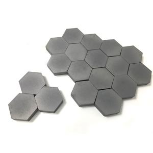
Silicon Carbide Ceramics: High-Performance Materials for Extreme Environment Applications sintered silicon nitride
1. Crystal Framework and Polytypism of Silicon Carbide
1.1 Cubic and Hexagonal Polytypes: From 3C to 6H and Past
(Silicon Carbide Ceramics)
Silicon carbide (SiC) is a covalently bound ceramic made up of silicon and carbon atoms set up in a tetrahedral control, creating one of one of the most complex systems of polytypism in products science.
Unlike a lot of ceramics with a single steady crystal structure, SiC exists in over 250 well-known polytypes– unique piling sequences of close-packed Si-C bilayers along the c-axis– ranging from cubic 3C-SiC (also known as β-SiC) to hexagonal 6H-SiC and rhombohedral 15R-SiC.
One of the most common polytypes made use of in engineering applications are 3C (cubic), 4H, and 6H (both hexagonal), each displaying slightly various electronic band frameworks and thermal conductivities.
3C-SiC, with its zinc blende framework, has the narrowest bandgap (~ 2.3 eV) and is typically grown on silicon substratums for semiconductor gadgets, while 4H-SiC provides premium electron movement and is preferred for high-power electronics.
The strong covalent bonding and directional nature of the Si– C bond provide remarkable firmness, thermal stability, and resistance to creep and chemical attack, making SiC suitable for extreme atmosphere applications.
1.2 Problems, Doping, and Electronic Properties
Regardless of its structural complexity, SiC can be doped to attain both n-type and p-type conductivity, enabling its usage in semiconductor devices.
Nitrogen and phosphorus work as contributor pollutants, presenting electrons into the conduction band, while light weight aluminum and boron function as acceptors, producing holes in the valence band.
Nonetheless, p-type doping efficiency is restricted by high activation energies, particularly in 4H-SiC, which presents challenges for bipolar tool style.
Native defects such as screw misplacements, micropipes, and piling faults can weaken gadget performance by functioning as recombination centers or leak courses, requiring top quality single-crystal growth for electronic applications.
The vast bandgap (2.3– 3.3 eV relying on polytype), high break down electric field (~ 3 MV/cm), and outstanding thermal conductivity (~ 3– 4 W/m · K for 4H-SiC) make SiC much above silicon in high-temperature, high-voltage, and high-frequency power electronic devices.
2. Handling and Microstructural Engineering
( Silicon Carbide Ceramics)
2.1 Sintering and Densification Methods
Silicon carbide is inherently challenging to densify as a result of its strong covalent bonding and reduced self-diffusion coefficients, requiring innovative processing methods to achieve complete thickness without additives or with marginal sintering help.
Pressureless sintering of submicron SiC powders is possible with the enhancement of boron and carbon, which promote densification by getting rid of oxide layers and improving solid-state diffusion.
Hot pushing uses uniaxial stress during home heating, enabling complete densification at lower temperature levels (~ 1800– 2000 ° C )and creating fine-grained, high-strength parts suitable for reducing tools and use components.
For big or complicated forms, response bonding is utilized, where porous carbon preforms are penetrated with molten silicon at ~ 1600 ° C, developing β-SiC sitting with very little shrinkage.
However, residual totally free silicon (~ 5– 10%) stays in the microstructure, restricting high-temperature efficiency and oxidation resistance above 1300 ° C.
2.2 Additive Production and Near-Net-Shape Construction
Recent advancements in additive production (AM), specifically binder jetting and stereolithography utilizing SiC powders or preceramic polymers, make it possible for the fabrication of complicated geometries formerly unattainable with traditional approaches.
In polymer-derived ceramic (PDC) paths, liquid SiC forerunners are shaped using 3D printing and then pyrolyzed at heats to produce amorphous or nanocrystalline SiC, usually needing additional densification.
These methods decrease machining costs and material waste, making SiC a lot more accessible for aerospace, nuclear, and heat exchanger applications where elaborate designs improve performance.
Post-processing steps such as chemical vapor seepage (CVI) or fluid silicon infiltration (LSI) are in some cases used to enhance thickness and mechanical integrity.
3. Mechanical, Thermal, and Environmental Efficiency
3.1 Strength, Hardness, and Wear Resistance
Silicon carbide rates amongst the hardest recognized products, with a Mohs firmness of ~ 9.5 and Vickers firmness going beyond 25 GPa, making it extremely resistant to abrasion, erosion, and damaging.
Its flexural strength usually varies from 300 to 600 MPa, relying on processing method and grain dimension, and it preserves toughness at temperature levels as much as 1400 ° C in inert atmospheres.
Crack strength, while modest (~ 3– 4 MPa · m 1ST/ TWO), suffices for many structural applications, especially when combined with fiber support in ceramic matrix composites (CMCs).
SiC-based CMCs are used in turbine blades, combustor liners, and brake systems, where they offer weight financial savings, gas performance, and extended life span over metal counterparts.
Its exceptional wear resistance makes SiC ideal for seals, bearings, pump elements, and ballistic shield, where toughness under harsh mechanical loading is critical.
3.2 Thermal Conductivity and Oxidation Security
Among SiC’s most important homes is its high thermal conductivity– approximately 490 W/m · K for single-crystal 4H-SiC and ~ 30– 120 W/m · K for polycrystalline forms– surpassing that of lots of metals and enabling effective heat dissipation.
This home is essential in power electronic devices, where SiC tools produce much less waste warmth and can operate at greater power thickness than silicon-based gadgets.
At raised temperatures in oxidizing settings, SiC creates a protective silica (SiO ₂) layer that slows down further oxidation, supplying good ecological durability approximately ~ 1600 ° C.
Nevertheless, in water vapor-rich environments, this layer can volatilize as Si(OH)FOUR, leading to sped up degradation– an essential obstacle in gas generator applications.
4. Advanced Applications in Energy, Electronics, and Aerospace
4.1 Power Electronic Devices and Semiconductor Devices
Silicon carbide has actually changed power electronic devices by allowing devices such as Schottky diodes, MOSFETs, and JFETs that run at greater voltages, frequencies, and temperatures than silicon equivalents.
These gadgets decrease energy losses in electric automobiles, renewable resource inverters, and commercial motor drives, adding to international power performance improvements.
The ability to operate at joint temperatures above 200 ° C enables simplified air conditioning systems and raised system integrity.
Furthermore, SiC wafers are made use of as substrates for gallium nitride (GaN) epitaxy in high-electron-mobility transistors (HEMTs), incorporating the benefits of both wide-bandgap semiconductors.
4.2 Nuclear, Aerospace, and Optical Solutions
In atomic power plants, SiC is a crucial part of accident-tolerant fuel cladding, where its low neutron absorption cross-section, radiation resistance, and high-temperature toughness boost security and performance.
In aerospace, SiC fiber-reinforced composites are utilized in jet engines and hypersonic vehicles for their lightweight and thermal security.
Furthermore, ultra-smooth SiC mirrors are used precede telescopes because of their high stiffness-to-density proportion, thermal security, and polishability to sub-nanometer roughness.
In recap, silicon carbide ceramics stand for a cornerstone of contemporary advanced products, integrating outstanding mechanical, thermal, and digital residential properties.
With exact control of polytype, microstructure, and processing, SiC continues to allow technological innovations in energy, transport, and severe atmosphere design.
5. Supplier
TRUNNANO is a supplier of Spherical Tungsten Powder with over 12 years of experience in nano-building energy conservation and nanotechnology development. It accepts payment via Credit Card, T/T, West Union and Paypal. Trunnano will ship the goods to customers overseas through FedEx, DHL, by air, or by sea. If you want to know more about Spherical Tungsten Powder, please feel free to contact us and send an inquiry(sales5@nanotrun.com).
Tags: silicon carbide ceramic,silicon carbide ceramic products, industry ceramic
All articles and pictures are from the Internet. If there are any copyright issues, please contact us in time to delete.
Inquiry us